From wafer metrology to printed circuit board inspection
Semiconductor device inspection
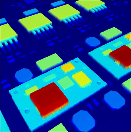
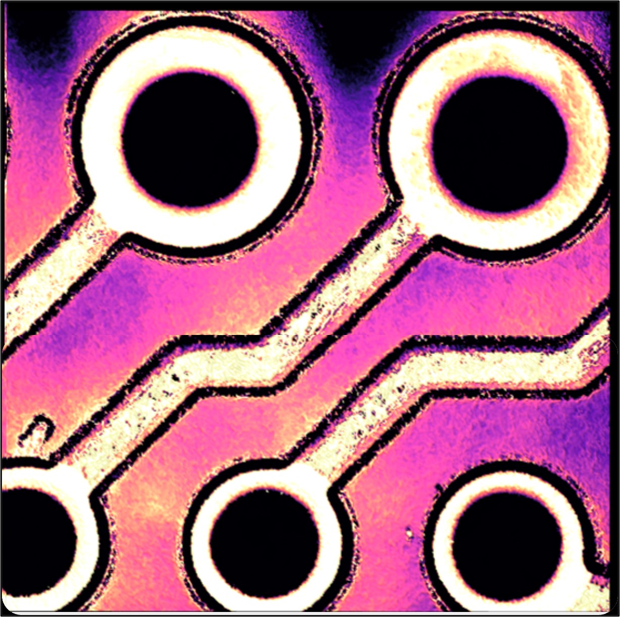
With their 1 μm resolution and 500 kHz acquisition speed, OptoComb 3D scanners go beyond the limits of conventional 2D inspection methods. They can measure in seconds the full 3D profile of printed circuit boards, including the smallest and most complex 3D features. Based on the high-accuracy 3D data of OptoComb, the automated inspection solutions offered by XTIA provide an instant assessment of the PCB dimensions and the 3D positioning of surface-mount devices. In addition, it also allows for the automated recognition of 3D microdefects such as scratches and particles.
As opposed to alternative optical methods, the interferential detection scheme of XTIA’s OptoComb sensors prevents the system from being affected by the ambient light. It makes OptoComb sensors ideal for use on the manufacturing floor in any light environment. It also allows for the measurement of both shiny and matt surfaces in the exact same conditions: metallic components (wiring, soldering) and non-metallic components can thus be fully scanned all at once.
Even semi-transparent objects such as semiconductor wafers can be measured with OptoComb 3D scanners. You can get insight into the morphology of the top wafer surface with a 1 μm resolution, extract its roughness or detect the presence of 3D microdefects. You can even measure the large curvature radius often encountered in hetero-epitaxial wafers.